Logic, Memory, Power: The Three Bottlenecks to Scaling AI Compute
Dylan Patel maps the three hard constraints on AI compute, and the picture is worse than the capex numbers suggest.
The standard framework for AI capacity lists four drivers: energy, compute, data, models. “Compute” is the one everyone mentions and few people unpack. What does it actually mean? What are the physical objects involved, who makes them, and what prevents us from simply building more? This is a quick overview of the concrete elements that make up the compute layer, and the bottlenecks that currently limit it.
The bottleneck keeps moving.
In 2023, the constraint was GPU availability itself. Nvidia’s H100, the chip that made large-scale model training commercially viable, had wait times of 36 to 52 weeks. Every major lab and cloud provider was fighting for allocation. In 2024, the GPU shortage eased, but a new problem surfaced: power and data centre capacity. Microsoft CEO Satya Nadella said publicly that the company had GPUs sitting in inventory it could not plug in, because the data centres lacked the electrical capacity to run them. Northern Virginia, the world’s largest data centre market, saw grid connection wait times stretch past three to five years. In 2025, as data centre construction caught up and operators found workarounds on power, the constraint shifted back upstream, to the semiconductor supply chain itself: the factories, the raw materials, and the machines that produce the chips.
Dylan Patel, founder of SemiAnalysis, the semiconductor research firm that has become the reference source on AI infrastructure economics, walked through this full picture on Dwarkesh Patel’s podcast. Patel’s argument is simple. The question is no longer how much money the hyperscalers (Amazon, Google, Microsoft, Meta, the handful of cloud giants that operate global-scale infrastructure) are willing to spend. It is how many chips the physical world can produce. $600 billion in combined Big Four capital expenditure this year does not translate into $600 billion of compute coming online this year. A large share covers turbine deposits for 2028, construction for 2027, and long-term power purchase agreements. The compute that actually becomes available is gated by silicon.
This is a supply-side version of something Vaclav Smil documents in Energy and Civilization: new energy sources do not diffuse at the speed of innovation. They diffuse at the speed of infrastructure replacement. Semiconductor fabs are the new power plants. Multi-year construction, single-supplier dependencies, demand that outruns deployment. Capital does not equal capacity.
Three constraints define the ceiling. All three involve Nvidia, which deserves a word of context.
Why Nvidia
Nvidia designs the GPUs (graphics processing units, repurposed from rendering video games to performing the massive parallel mathematical operations that AI training and inference require) that power the vast majority of the world’s AI infrastructure. Their dominance is near-total in frontier AI: an estimated 80 to 90% market share in data centre AI chips. The company does not manufacture its own chips. It designs them and contracts production to TSMC (Taiwan Semiconductor Manufacturing Company), the Taiwanese foundry that fabricates the world’s most advanced semiconductors.
Nvidia’s dominance is not only about hardware. It also rests on CUDA, the software platform that sits between the GPU hardware and the applications that run on it. CUDA provides the programming tools, libraries, and optimised routines that allow researchers and engineers to write AI code for Nvidia chips. It has been in development since 2006, and nearly all major AI frameworks (PyTorch, TensorFlow) are built on top of it. This creates deep lock-in: even when a competitor produces a chip with comparable raw performance, migrating away from CUDA means rewriting and re-optimising an entire software stack. It is one of the strongest ecosystem moats in the industry.
Nvidia’s product line has been on an aggressive annual release cycle since 2022. The Hopper architecture (H100, released 2022) made large-scale transformer training feasible at commercial scale. Blackwell (B200, announced March 2024, shipping in volume since late 2024) delivered roughly 4x the training performance of Hopper and introduced support for FP4 precision, dramatically improving inference throughput. Vera Rubin, announced at GTC 2025, is the next full architectural leap: 50 petaflops of FP4 inference (2.5x Blackwell), fabricated on TSMC’s 3 nm process, paired with next-generation HBM4 memory. Rubin enters mass production in Q3/Q4 2026.
Each generation roughly triples performance while increasing price by 50 to 100%. Jensen Huang calls this “ultimate Moore’s Law”. Patel’s point is that the pace of architectural improvement now runs faster than the pace at which the supply chain can produce the chips.
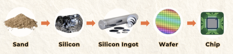
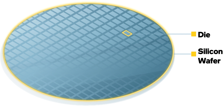
Bottleneck 1: Logic wafers
A wafer is a thin disc of pure silicon, roughly the size of a dinner plate (30 cm across). Using photolithography, a process that projects patterns of light onto the silicon surface to create microscopic structures, hundreds of identical chip circuits are printed onto the wafer simultaneously. Each individual circuit is then cut out of the disc. That small square of silicon, carrying millions or billions of transistors, is called a die. A GPU like the Blackwell B200 uses two of these dies bonded together in a single package, totalling 208 billion transistors.
TSMC’s N3 node, its most advanced manufacturing process (3 nanometre feature size), produces the dies for both Blackwell and the upcoming Rubin. This node is effectively sold out through 2027. Nvidia has secured over 70% of N3 wafer allocation by next year, having committed early and aggressively while competitors hesitated. Google, by Patel’s account, was slow to recognise how fast its inference revenue would scale. Its Gemini product generated negligible revenue through Q3 2024, then suddenly hit $5 billion ARR in Q4. By the time Google went back to TSMC to increase its orders, capacity was committed. The result is an allocation game in which commitment timing, not engineering talent, determines who gets to train and serve frontier models. This is part of why Google invested heavily in developing its own TPU (Tensor Processing Unit) chip line, co-designed with Broadcom and also fabricated at TSMC: to reduce its dependency on Nvidia allocation. Google has committed over a million TPUs to Anthropic alone, and is now exploring TPU sales to other companies. But TPUs still compete for the same scarce TSMC fab capacity, so the underlying constraint remains.
This has consequences further down the stack. TSMC builds new fabs (the ultra-clean fabrication plants where wafers are processed, costing $20 billion or more each) on two-to-three-year cycles. A data centre goes up in eight months. Even if power and cooling were infinite tomorrow, chip supply would still cap deployment.
And beneath TSMC sits the ultimate chokepoint: ASML, the Dutch company that holds a global monopoly on EUV (extreme ultraviolet) lithography. These are the machines that use focused light at 13.5 nm wavelength to print transistor patterns onto wafers at nanometre scale. Each machine costs $300 to $400 million, contains over 100,000 components, and must be assembled, tested, disassembled for shipping, then reassembled on site. ASML can produce roughly 70 per year today. Under aggressive expansion, perhaps 100 by decade’s end.
To put that number in perspective: at approximately 3.5 EUV machines per gigawatt of AI chip capacity, that puts a hard upper bound of around 200 GW of total cumulative AI compute by 2030. But EUV machines do not only serve AI. They produce the leading-edge chips in smartphones (Apple’s A-series and M-series), laptops, game consoles, automotive processors, and virtually every other device that uses advanced silicon. AI’s share of EUV capacity has been growing fast (Nvidia overtook Apple as TSMC’s largest customer in 2025), but it remains one claimant among several. This is the deeper tension: even as hyperscalers pour hundreds of billions into data centres and power, the actual compute they can deploy is capped by a supply chain that serves the entire global electronics industry. The money is there. The machines are not. ASML’s EUV backlog hit $38.8 billion by Q4 2025.
Bottleneck 2: Memory
The second constraint is high-bandwidth memory. To understand why, a quick detour through chip anatomy.
A GPU needs two things to work: processing cores (which do the computation) and memory (which stores the data the cores are working on). The speed at which data can move between memory and cores, the memory bandwidth, is often the real performance limiter. Standard DDR DRAM, the commodity memory in phones and laptops, is too slow for AI workloads. So Nvidia’s data centre GPUs use HBM (high-bandwidth memory): multiple DRAM layers stacked vertically and bonded together with thousands of through-silicon vias, delivering massive bandwidth. Each new generation of GPU ships with more HBM and faster bandwidth, and Rubin will be the first to use HBM4, the next-generation standard.
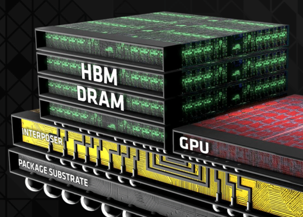
The trade-off is in the manufacturing. HBM stacking requires roughly four times the wafer area per gigabyte compared to standard DRAM. Every HBM stack shipped to a data centre therefore crowds out the commodity memory that goes into phones, laptops, and cars. All three major memory vendors, SK Hynix, Samsung, and Micron, are sold out through 2026. DRAM contract prices rose 90 to 95% quarter on quarter in Q1 2026. IDC projects the largest decline in smartphone shipments in over a decade (minus 12.9% in 2026). Micron exited its consumer Crucial brand entirely in late 2025, redirecting all capacity toward higher-margin AI memory. SemiAnalysis covers the full dynamics in Memory Mania and in their HBM roadmap analysis.
Memory now represents roughly 30% of hyperscaler capex. And the mechanism is self-reinforcing: each generation of AI accelerator ships with more HBM, model designers immediately fill it with larger parameter counts and longer context windows, and the memory wall reasserts itself within months. This is not a temporary squeeze. As long as model architectures keep scaling, memory will remain binding.
The downstream effects go well beyond AI. The consumer electronics industry is being priced out of its own supply chain by higher-margin data centre demand. This is a theme we return to often: AI scaling is not merely an engineering challenge. It is a resource allocation problem with consequences that spill across markets and geographies.
Bottleneck 3: Power
The third constraint, power, is the one Patel is most relaxed about, at least in the US. Data centre operators have moved to “post-meter” solutions: on-site gas turbines, fuel cells, and even repurposed jet engines that bypass the grid entirely. Permitting and grid interconnection remain slow, but the physical energy is available. The US added roughly 20 GW of incremental AI data centre capacity this year. For reference, a single gigawatt powers roughly 700,000 homes.
Power matters, but it sits lower in the constraint hierarchy than chips. You can build a data centre faster than you can build a fab, and you can source electricity faster than you can source an EUV machine. That said, Patel’s sanguinity deserves context: the IEA projects global data centre electricity demand doubling to 945 TWh by 2030, with real implications for grid stability and carbon budgets, particularly outside the US, in regions without abundant clean baseload. The entanglement between AI and energy is one of the defining tensions of this technological cycle, and one we explored at length in our deep dive on Vaclav Smil’s Energy and Civilization: every major civilisational transition has been paced by energy infrastructure, and this one will be no different.
What this means
Two takeaways worth keeping in mind when thinking about the bottom of the AI capacity stack.
The first is about positioning between the labs. OpenAI signed aggressive, long-term compute contracts, even when the market doubted its ability to pay for them. Anthropic, more conservative by design, now faces a scramble for capacity at a moment when its revenue is scaling faster than its infrastructure. Patel estimates both labs will reach five to six gigawatts by year-end, but through very different paths. OpenAI arrives through locked-in deals at historic pricing. Anthropic arrives through a patchwork of hyperscaler partnerships, neoclouds (the new generation of GPU-focused cloud providers: CoreWeave, Nebius, NScale), and revenue-share arrangements at higher effective cost. Anthropic’s $50 billion infrastructure deal with Fluidstack, announced in late 2025, is a case in point: custom data centres in Texas and New York, coming online throughout 2026, built by a neocloud founded in 2017 that also serves Meta and Mistral. Fluidstack was chosen for speed, the ability to deliver gigawatts of power on short timelines, precisely because the established hyperscalers had no remaining capacity to offer. The difference in long-run unit economics between labs that locked in compute early and those assembling it on the fly could be substantial.
The second insight is about GPU depreciation, and it is counterintuitive. In a compute-constrained world, an H100 is worth more today than when it shipped. Not because the hardware improved, but because the models it can serve are more capable, and therefore more valuable per token, than the models that existed at launch. Dwarkesh frames this through the Alchian-Allen effect, an economics principle: when a fixed cost is added to goods of different quality, the premium good becomes relatively cheaper. Applied to AI: if an H100 goes from $2/hour to $3/hour, but Opus produces one million tokens while Sonnet produces two million, the effective premium for frontier quality shrinks. The fixed cost increase pushes all demand toward the best available model. Long-term compute contracts signed at 2023 or 2024 pricing now carry enormous embedded margin advantages. This is the same logic that governs energy infrastructure lock-in, as Smil documents at length: whoever commits to the dominant regime early captures decades of structural advantage.
The broader picture is that, in this cycle, durable advantage may sit in semiconductor supply chain positioning rather than in model architecture. The companies that secured capacity early, committed capital ahead of revenue, and locked in multi-year contracts are the ones best positioned to capture margin as inference demand scales. The rest are competing for scraps at spot pricing. The verification frontier remains a real constraint on how quickly that demand translates into enterprise revenue. But the supply-side ceiling is now the binding variable.